- 您现在的位置:买卖IC网 > Sheet目录487 > NTD4913NT4G (ON Semiconductor)MOSFET N-CH 30V 32A DPAK
NTD4913N
Power MOSFET
30 V, 32 A, Single N ? Channel, DPAK/IPAK
Features
? Low R DS(on) to Minimize Conduction Losses
? Low Capacitance to Minimize Driver Losses
? Optimized Gate Charge to Minimize Switching Losses
? These are Pb ? Free Devices
Applications
? CPU Power Delivery
? DC ? DC Converters
V (BR)DSS
30 V
http://onsemi.com
R DS(ON) MAX
10.5 m W @ 10 V
15 m W @ 4.5 V
I D MAX
32 A
D
MAXIMUM RATINGS (T J = 25 ° C unless otherwise stated)
Parameter
Symbol
Value
Unit
Drain ? to ? Source Voltage
Gate ? to ? Source Voltage
V DSS
V GS
30
± 20
V
V
G
2 3
3
3
Continuous Drain
Current R q JA
(Note 1)
Power Dissipation
R q JA (Note 1)
Continuous Drain
Current R q JA
(Note 2)
Power Dissipation
R q JA (Note 2)
Continuous Drain
Current R q JC
(Note 1)
Power Dissipation
R q JC (Note 1)
Pulsed Drain
Current
Steady
State
t p =10 m s
T A = 25 ° C
T A = 100 ° C
T A = 25 ° C
T A = 25 ° C
T A = 100 ° C
T A = 25 ° C
T C = 25 ° C
T C = 100 ° C
T C = 25 ° C
T A = 25 ° C
I D
P D
I D
P D
I D
P D
I DM
10.5
7.4
2.5
7.7
5.4
1.36
32
23
24
132
A
W
A
W
A
W
A
1 2 1
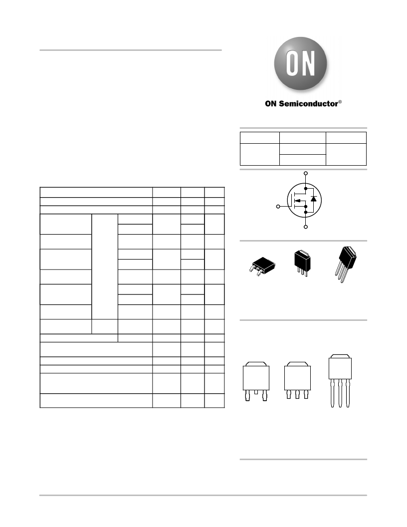
STYLE 2 DPAK)
S
N ? CHANNEL MOSFET
4 4
4
1
2
CASE 369AA CASE 369AC CASE 369D
DPAK 3 IPAK IPAK
(Bent Lead) (Straight Lead) (Straight Lead
MARKING DIAGRAMS
Current Limited by Package
T A = 25 ° C
I DmaxPkg
60
A
& PIN ASSIGNMENTS
Operating Junction and Storage
Temperature
Source Current (Body Diode)
T J ,
T STG
I S
? 55 to
+175
20
° C
A
4
Drain
4
Drain
4
Drain
Drain to Source dV/dt
Single Pulse Drain ? to ? Source Avalanche
Energy (T J = 25 ° C, V DD = 50 V, V GS = 10 V,
I L = 21 A pk , L = 0.1 mH, R G = 25 W)
dV/dt
EAS
8.0
22
V/ns
mJ
1
2
3
Source Gate Drain Source
1
2
3
Lead Temperature for Soldering Purposes T L 260 ° C
(1/8” from case for 10 s)
Stresses exceeding Maximum Ratings may damage the device. Maximum
Ratings are stress ratings only. Functional operation above the Recommended
Operating Conditions is not implied. Extended exposure to stresses above the
Recommended Operating Conditions may affect device reliability.
1. Surface ? mounted on FR4 board using 1 sq ? in pad, 1 oz Cu.
2. Surface ? mounted on FR4 board using the minimum recommended pad size.
2
1 Drain 3
Gate
Y = Year
WW = Work Week
4913N = Device Code
Gate Drain Source
G
= Pb ? Free Package
ORDERING INFORMATION
See detailed ordering and shipping information in the package
dimensions section on page 3 of this data sheet.
? Semiconductor Components Industries, LLC, 2010
June, 2010 ? Rev. 1
1
Publication Order Number:
NTD4913N/D
发布紧急采购,3分钟左右您将得到回复。
相关PDF资料
NTD4959NT4G
MOSFET N-CH 30V 9A TP-FA
NTD4960NT4G
MOSFET N-CH 30V 11.1A DPAK
NTD4965NT4G
MOSFET N-CH 30V 68A DPAK
NTD4970N-35G
MOSFET N-CH 30V 38A IPAK
NTD50N03RT4G
MOSFET N-CH 25V 7.8A DPAK
NTD5413NT4G
MOSFET N-CH 60V 30A DPAK
NTD5414NT4G
MOSFET N-CH 60V 24A DPAK
NTD5802NT4G
MOSFET N-CH 40V 16.4A DPAK
相关代理商/技术参数
NTD4959N
制造商:ONSEMI 制造商全称:ON Semiconductor 功能描述:Power MOSFET 30 V, 58 A, Single N−Channel, DPAK/IPAK
NTD4959N-1G
功能描述:MOSFET NFET DPAK 30V RoHS:否 制造商:STMicroelectronics 晶体管极性:N-Channel 汲极/源极击穿电压:650 V 闸/源击穿电压:25 V 漏极连续电流:130 A 电阻汲极/源极 RDS(导通):0.014 Ohms 配置:Single 最大工作温度: 安装风格:Through Hole 封装 / 箱体:Max247 封装:Tube
NTD4959N-35G
功能描述:MOSFET NFET DPAK 30V RoHS:否 制造商:STMicroelectronics 晶体管极性:N-Channel 汲极/源极击穿电压:650 V 闸/源击穿电压:25 V 漏极连续电流:130 A 电阻汲极/源极 RDS(导通):0.014 Ohms 配置:Single 最大工作温度: 安装风格:Through Hole 封装 / 箱体:Max247 封装:Tube
NTD4959NH
制造商:ONSEMI 制造商全称:ON Semiconductor 功能描述:Power MOSFET 30 V, 58 A, Single N−Channel, DPAK/IPAK
NTD4959NH-1G
功能描述:MOSFET NFET DPAK 30V RoHS:否 制造商:STMicroelectronics 晶体管极性:N-Channel 汲极/源极击穿电压:650 V 闸/源击穿电压:25 V 漏极连续电流:130 A 电阻汲极/源极 RDS(导通):0.014 Ohms 配置:Single 最大工作温度: 安装风格:Through Hole 封装 / 箱体:Max247 封装:Tube
NTD4959NH-35G
功能描述:MOSFET NFET DPAK 30V RoHS:否 制造商:STMicroelectronics 晶体管极性:N-Channel 汲极/源极击穿电压:650 V 闸/源击穿电压:25 V 漏极连续电流:130 A 电阻汲极/源极 RDS(导通):0.014 Ohms 配置:Single 最大工作温度: 安装风格:Through Hole 封装 / 箱体:Max247 封装:Tube
NTD4959NHT4G
功能描述:MOSFET NFET DPAK 30V RoHS:否 制造商:STMicroelectronics 晶体管极性:N-Channel 汲极/源极击穿电压:650 V 闸/源击穿电压:25 V 漏极连续电流:130 A 电阻汲极/源极 RDS(导通):0.014 Ohms 配置:Single 最大工作温度: 安装风格:Through Hole 封装 / 箱体:Max247 封装:Tube
NTD4959NT4G
功能描述:MOSFET NFET DPAK 30V RoHS:否 制造商:STMicroelectronics 晶体管极性:N-Channel 汲极/源极击穿电压:650 V 闸/源击穿电压:25 V 漏极连续电流:130 A 电阻汲极/源极 RDS(导通):0.014 Ohms 配置:Single 最大工作温度: 安装风格:Through Hole 封装 / 箱体:Max247 封装:Tube
